Understand Your Materials –
See what’s happening beneath the surface
At Secat, we give you a complete picture of your materials — from microstructure to performance. Our hands-on characterization services provide actionable insights that help you optimize alloys, improve processes, and develop high-performing products.
Our Lexington laboratory offers state-of-the-art facilities for materials testing and development, giving you the tools to evaluate, refine, and advance your products with confidence.

Why Characterization Matters
Every piece of metal tells a story. Through advanced characterization techniques, Secat helps you uncover what’s happening beneath the surface — so you can make informed decisions, solve production challenges, and develop better materials.
Benefits of Materials Characterization Testing:
-
Evaluate quality and consistency of materials
-
Detect and understand defects or failures
-
Support process improvement and R&D
-
Validate supplier materials and heat treatments
-
Document compliance with standards or specs
Materials Characterization Services
Microstructural Analysis
-
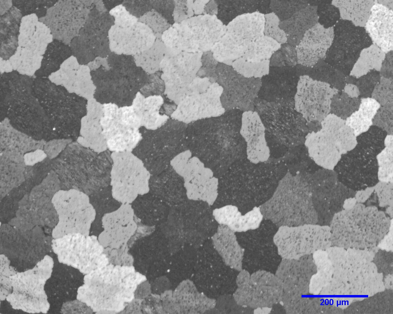
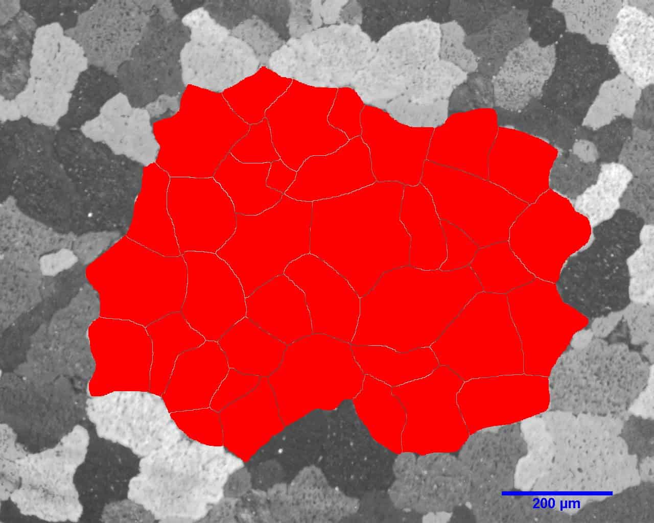
Optical Microscopy: Examine grain structure, phase distribution, and surface features.
-
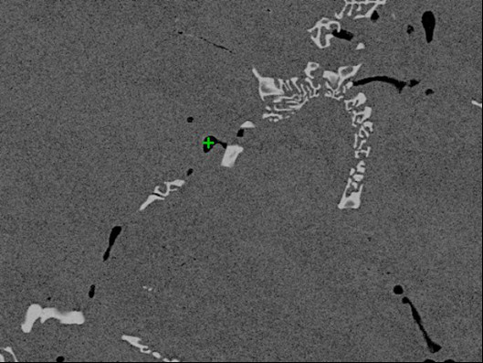
Scanning Electron Microscopy (SEM): High-resolution imaging for detailed surface morphology and elemental analysis.
-
Transmission Electron Microscopy (TEM): Nanoscale examination of internal structures and interfaces.
Elemental and Phase Composition
-
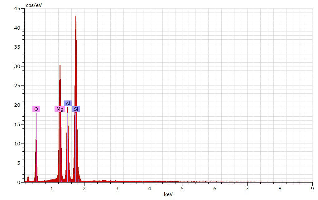
Energy Dispersive X-ray Spectroscopy (EDS): Elemental mapping and quantification.
-
X-ray Diffraction (XRD): Phase identification and crystallographic analysis.
-
X-ray Photoelectron Spectroscopy (XPS): Surface chemical state and composition profiling.
Thermal and Surface Analysis
-
Differential Scanning Calorimetry (DSC): Thermal transitions and stability.
-
Thermogravimetric Analysis (TGA): Decomposition and thermal stability.
Weld & Joint Evaluation
-
Analyze weld quality, interfaces, and defects to ensure integrity and performance in fabricated assemblies.
Investigation Examples
Grain Size Evaluation
Particle Size Evaluation
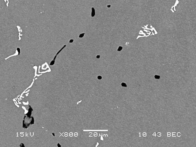
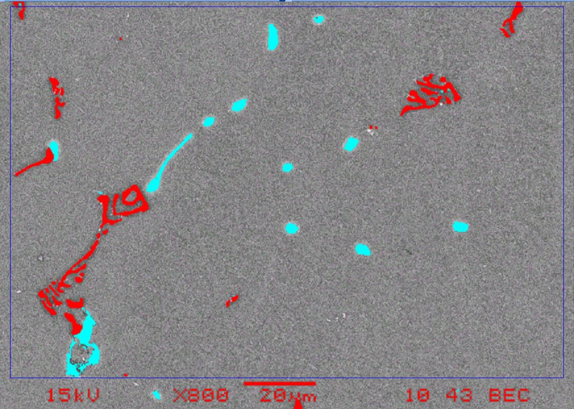
Particle Size Evaluation
SEM/EDS