The Electron Microscopy Center at the University of Kentucky, located a short distance from Secat in Lexington, KY, recently acquired a state-of- the-art focused ion beam and scanning electron microscope (FIB-SEM) system. This instrument, a Helios NanoLab 660 made by FEI, offers a suite of characterization capabilities for advanced analysis of materials. The Electron Microscopy Center provides both
training and full characterization services to internal users and external customers.
The SEM and FIB are combined in a single chamber, and the SEM offers a spatial resolution better than 1 nm. In practice, this allows the imaging of features as small as 1-2 nm, even when the sample is non-conducting. Multiple detectors,
each of which generates different contrast and yields complementary sample
information, can be selected for imaging. In addition to the traditional modes of
secondary electron imaging and backscattered electron imaging, the system can produce images with ions or with filtered electrons (removal of stray electrons). It
is possible to obtain clear contrast between grains, simply due to crystallographic
orientation.
The focused ion beam (FIB) portion of this system utilizes a gallium ion source to produce a narrow beam of ions that mill material from the sample surface, with
2.5 nanometer spatial resolution. At higher beam current, sample volumes up to
10 or 100 microns in each dimension can be removed. Cross-sections can be easily milled into a sample surface, revealing interior regions for imaging and also analysis of chemistry or grain orientation. The x-ray energy dispersive
spectrometer (EDS) has a large area detector that facilitates rapid chemical
analysis of sample composition. Also, the electron backscatter detector (EBSD)
determines orientation of grains within the sample, at a resolution down to 10-20
nm.
The FIB-SEM system includes automated software for the acquisition of images/composition/orientation over
large sample areas. Analysis runs can be
scheduled for overnight acquisition, generating maps that cover millimeter
dimensions that still have high resolution.
A distinct advantage of the FIB-SEM is the ability to perform site-specific
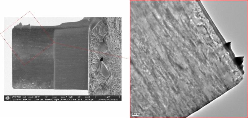
characterization of specimen features. Once the overall sample surface has been surveyed, specific features can be selected for cross-sectional analysis. Moreover, thin foils can be milled from a particular site and extracted for analysis in the transmission electron microscope. This permits the characterization of specific grains, phases, inclusions, etc. The milling capabilities of the FIB-SEM also allow a cross-section to be successively milled in small steps, with imaging/analysis after each cross-sectional slice, after which the slices can be reconstructed to produce a three-dimensional tomograph that includes information throughout the analyzed volume.
Selected results for aluminum are presented below. Of course, these characterization techniques can be applied to all metals, alloys and other
materials. In fact, the ability to image at low beam voltage allows non-conducting
materials to be analyzed without the need for sample coating.
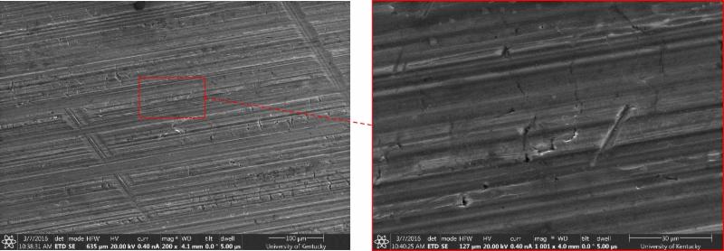
High resolution imaging of the surface of an aluminum sheet sample.
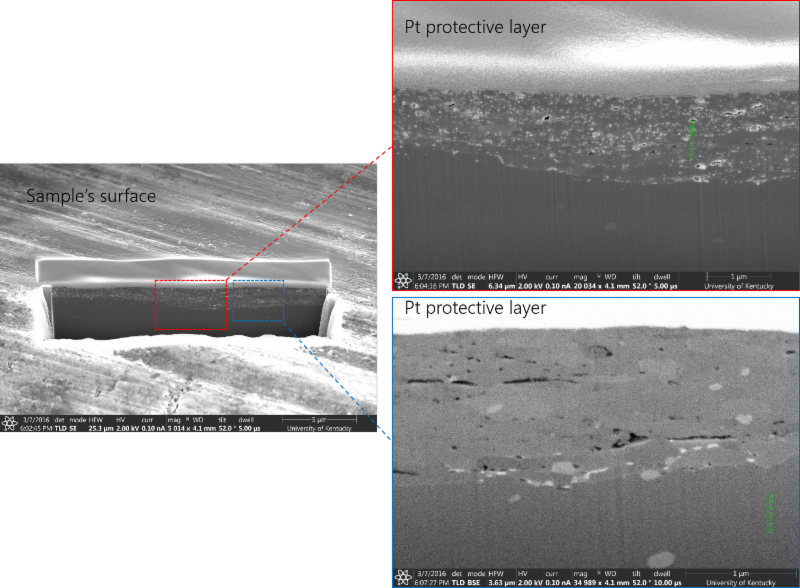
Cross-section of an aluminum sheet sample (left); secondary electron (top right)
and backscattered electron (bottom right) images of the defect-rich subsurface.
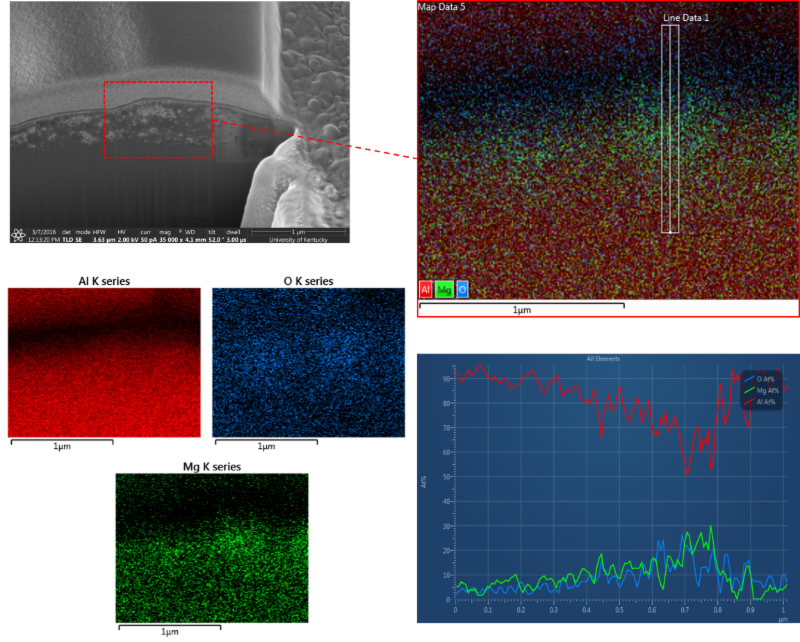
FIB cross-section and EDS map of composition for the subsurface of an aluminum sample. The FIB was used to mill a cross-section at the region of interest (top left), and the chemical map revealed a layer rich in oxygen and magnesium just beneath the surface (top right). A composition depth profile across this region confirms its concentration and size (bottom right).


